


Tantalum sputtering target is a high-performance rare metal target material, critical for semiconductor chips, optical coating and microelectronic component manufacturing.
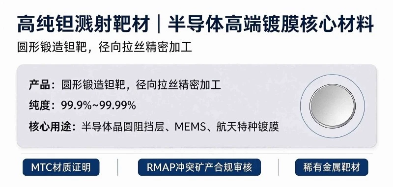
The round high-purity tantalum target shown in the picture is produced by forging and precision machining with radial wire drawing surface. It features high purity, high density, uniform grain structure and low impurity level, meeting strict requirements for wafer fabrication and thin-film deposition processes.
Core Product Advantages
✅ High purity: Available from 99.9% up to 99.99%, strictly controlled impurities including oxygen, carbon and iron
✅ Excellent density: Forged raw material, free of internal porosity or delamination for stable thin-film deposition
✅ Precision machining: Customizable diameter & thickness, controllable flatness & surface roughness; copper backing plate bonding service available
✅ Compliance support: MTC material test certificate available, RMAP conflict mineral audit supported, meeting EU & US supply chain due diligence rules
Main Application Fields
Semiconductor: Barrier layer thin film for memory chips & logic ICs
Microelectronics: Thin film coating for capacitors, sensors and MEMS devices
High-end optics, vacuum coating, aerospace & military special coatings
Industry Outlook: Tantalum is a national strategic rare metal. Driven by global semiconductor capacity expansion and advanced packaging demand, overseas demand for high-purity tantalum targets keeps rising. Supply chain security, material purity and compliance documentation have become key evaluation criteria for international buyers.
Disclaimer: This is industry product information for business reference only, not a purchasing commitment.
Foreign-Trade Keywords
Tantalum sputtering target, high purity tantalum, semiconductor thin film, wafer barrier layer, rare metal target, RMAP conflict mineral, MTC certificate, vacuum coating


