




Tungsten Sputtering Target
2.Product Name:Tungsten Sputtering Target
3.Element Symbol:W
4.Purity:3N5
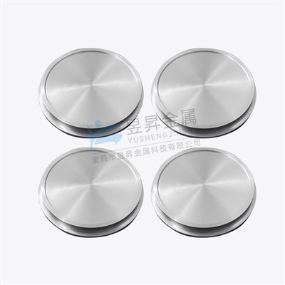
5.Shape:Planar target, Rotary target
Product Introduction
High-purity tungsten for sputtering targets is inherently brittle and difficult to machine. When produced with ultra-high purity, tungsten retains hardness superior to many steels while gaining sufficient ductility for forming via forging, drawing or extrusion. Sintering is also a common forming method for tungsten components.
Among all pure metals, tungsten boasts the highest melting point (3422°C / 6192°F), lowest vapor pressure (above 1650°C / 3000°F), highest tensile strength and minimum thermal expansion coefficient. These outstanding properties originate from strong covalent bonds formed by 5d electrons between tungsten atoms. Small additions of tungsten can greatly improve the durability of steel.
Yusheng Metal specializes in manufacturing tungsten sputtering targets in various shapes and purity grades, mainly serving the semiconductor and microelectronics industries. Thanks to its ultra-high melting point, tungsten thin films applied in TFT-LCD thin-film transistors remain highly stable under high-temperature conditions. Our exclusive forming technology delivers targets with high density, fine average grain size and high purity. It supports faster sputtering rates and forms highly uniform tungsten films.
Our flexible production process can tailor the microstructure to meet your requirements. Uniformly oriented grains ensure stable erosion rate and homogeneous deposited layers. The typical grain size is 100 μm.
High chemical purity is critical for metal sputtering targets. High-purity tungsten targets produce thin films with better electrical conductivity and fewer particles generated during PVD deposition.
Metallic elements test method: GDMS & ICP-OES
Gas components test method: LECO
Manufacturing Process
General workflow: Material preparation → Powder mixing → Cold isostatic pressing → Sintering → Rolling → Annealing → Metallographic inspection → Machining → 3D dimensional inspection → Cleaning → Final inspection → Packaging & Shipment
Detailed process parameters for standard tungsten target (purity ≥99.95%):
Tungsten powder blending
Cold isostatic pressing, holding 5–10 min
Intermediate frequency induction sintering at 2300–2400°C for 8–12 h
Annealing at 1550°C for 90–180 min
Multi-pass hot rolling down to 5–15 mm thickness, total deformation >60%
Secondary annealing at 1300–1400°C for 90–150 min
Precision machining, surface machining allowance ~1.5 mm
This route produces tungsten targets with stable performance and good machinability, without relying on high-cost equipment.
Core Advantages
Highest melting point, low vapor pressure, low thermal expansion
High density, controllable grain structure, typical grain size 100 μm
Stable sputtering speed, consistent erosion rate, uniform tungsten thin film
High purity, fewer particles, excellent conductivity of deposited films
Customizable microstructure, planar / rotary targets available

Applications
Semiconductor and microelectronics
TFT-LCD thin film transistor layers
Vacuum coating, PVD thin film deposition
High-temperature functional thin film systems
Available Tungsten Alloy Targets
We also supply various tungsten alloy sputtering targets: Tungsten-Titanium (WTi), Tungsten-Copper (WCu), Tungsten-Manganese (WMn), Tungsten-Nickel (WNi)
FAQ
Q1: What is the melting point of pure tungsten?
A: 3422°C, the highest among all pure metals.
Q2: What testing methods are used for purity inspection?
A: GDMS and ICP-OES for metallic impurities; LECO for gas element analysis.
Q3: Can you supply tungsten alloy sputtering targets?
A: Yes, WTi, WCu, WMn, WNi and other tungsten alloy targets are available.
Q4: What is the typical grain size of your tungsten sputtering target?
A: Typical grain size is 100 μm.
Hot Tags: tungsten sputtering target, suppliers, manufacturers, factory, customized, buy, price, quotation, quality, for sale, in stock
Next
Tungsten TargetYou Might Also Like




Send Inquiry