


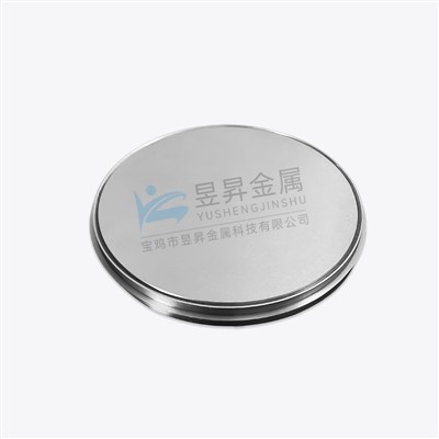
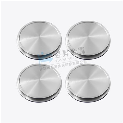
Tungsten Titanium Sputtering Targets
2.Product Name:Tungsten Titanium Sputtering Targets
3.Element Symbol:W + Ti
4.Purity:3N5, 4N, 4N5
5.Shape:Planar
Tungsten Titanium Sputtering Targets:
Our Tungsten Titanium Sputtering Targets are produced using cutting-edge powder metallurgical manufacturing techniques. We offer WTi sputtering targets in a range of sizes, up to 400 millimeters in diameter. We are among the first manufacturers to create WTi as both a rotary target and a planar target. The titanium content of our WTi targets is usually 10% by weight.
| Density | ≥ 98% |
| Purity | > 99.95% |
| Titanium content | 10% by weight |
| Homogeneity of titanium distribution | ± 0.5% |
| Microstructure | Fine grain, < 50 µm grain size |
 Tungsten-titanium Sputtering Targets
 Tungsten-titanium alloy
Application areas for tungsten-titanium:
Tungsten-titanium (WTi), which contains 10% titanium by weight, is used as a metallization glue and diffusion barrier in microchips. In this case, WTi is used to separate the metallization and semiconductor layers, such as copper from silicon or aluminum from silicon. Without diffusion barriers, silicon and copper would combine to create an intermetallic phase in microchips, which would compromise the semiconductor's performance. A WTi barrier layer is used in flexible thin-film solar cells (CIGS) to stop iron ions from diffusing through the molybdenum back contact and into the semiconductor. The efficiency of CIGS solar cells can be greatly decreased by as little as a few g/g of iron.
a.Powder metallurgy is used to create tungsten titanium sputtering targets, which are extensively used in semiconductor and thin-film solar cell manufacturing.
b.WTi10wt% thin film is used in semiconductor applications as an adhesion layer and diffusion barrier to isolate the metallization layers from the semiconductor, such as copper or aluminum from silicon. As a result, the transistor function in microchips can be greatly enhanced.
c.WTi10wt% thin film is also used in thin film solar cells as a barrier layer to stop iron ions from diffusing from the steel substrate to the molybdenum back contact and CIGS semiconductor.Targets made of tungsten titanium are also used to cover tools and LEDs.
In the two figures, a flip chip semiconductor metallization using WTi layers is shown below the schematic construction of a CIGS solar cell on the left.


The quality of the layer increases with coating substance purity. To ensure the greatest level of material purity, we only use the purest powder and mix it in our own facilities from the beginning. From the powder to the finished product, we closely watch each stage to make sure that only targets with the precise guaranteed density, purity, and a homogeneous microstructure leave our facility.
Our factory is capable of manufacturing targets with WTi 90/10wt%, WTi 85/15wt%, and special composition Tungsten Titanium Sputtering Targets that can be customized. The density of the actual targets is > 99%, and the typical grain size is 100um. End users can achieve constant erosion rates and high purity and homogeneous thin film coating during PVD process with up to 4N5 purity and special annealing treatment, uniform grain size, and reduced gas content.
If you have any needs or questions, please feel free to contact us.

CONTACT US
Sales Manager:
Contact: Li Fengwu
Email: kd@tantalumysjs.com
Tel: 13379388917
Fax: 0917-3139100
Post code: 721013
Web:https://www.tantalumysjs.com/
Add:Wenquan village Industrial Zone, Gaoxin Development Zone, Baoji City, Shaanxi Province, China
Hot Tags: tungsten titanium sputtering targets, suppliers, manufacturers, factory, customized, buy, price, quotation, quality, for sale, in stock
Previous
Tungsten RoundYou Might Also Like


Send Inquiry