




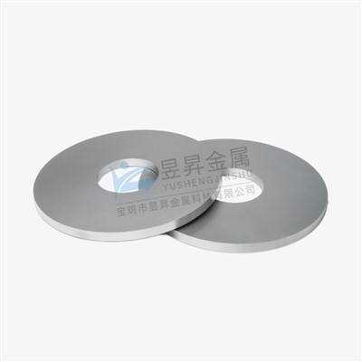
Ta Sputter Target
2.Grade:R05200 R05400 R05252 (Ta-2.5W) R05255 (Ta-10W)
3.Purity:≥99.95% (Maximum 99.99%)
4.Recrystalize: Minimum 95%
5.Grain Size:Minimum 40um
6.Surface Roughness:Maximum Ra0.4
7.Flatness:0.1mm or maximum 0.10%
8.Tolerance:Diameter +/-0.254mm
Product Basic Introduction
Yusheng Metal tantalum sputtering targets are manufactured from tantalum ingots via EB electron beam melting, rolling and annealing processes. Targets produced by this process feature uniform crystal structure, consistent texture and even energy distribution, with sound internal microstructure.
Benefiting from the continuous expansion of the IC industry and the development of high-density chip processes, tantalum has become a key sputtering material for diffusion barrier layers in copper interconnect technology by virtue of outstanding chemical stability. The microstructure uniformity of tantalum targets directly determines sputtering stability and thin-film quality.
Tantalum targets are required to have fine, uniform grains and random grain orientation to achieve excellent thin-film forming performance. Nevertheless, tantalum is prone to forming preferred texture during cold working: core region with <111>//ND orientation and surface with <100>//ND orientation. This anisotropic texture will cause varied sputtering rate along target thickness, and destabilize the sputtering process.
Tantalum can form dense, protective oxide films, which makes it widely applied for electrolytic capacitors. Early tantalum thin-film deposition relied on evaporation. Since the late 1960s, sputtering and other PVD technologies have gradually replaced evaporation, becoming the mainstream thin-film deposition method.
The working principle of magnetron sputtering: In vacuum environment, ionized argon ions are accelerated by electromagnetic fields to bombard the tantalum target surface. The bombardment knocks out tantalum atoms, which then travel and deposit onto the substrate to form a functional tantalum thin film.
Product reference link:https://www.tantalumysjs.com/products
Production Flow
EB electron beam melting → tantalum ingot preparation → rolling → annealing → precision machining → inspection → backing bonding (optional) → finished target
Core Advantages
EB melting + controlled rolling & annealing process Realize well-regulated crystal structure and texture, reduce internal defects, and deliver stable internal structure.
Focus on texture control We optimize rolling and annealing parameters to suppress the formation of strong <111> / <100> preferred orientation, reduce anisotropy, and avoid sputtering rate fluctuation with target consumption.
Stable sputtering performance for copper barrier layer Fine and uniform grains guarantee consistent erosion rate, fewer particles and stable thin-film quality for IC copper interconnect diffusion barrier layers.
Wide application compatibility Suitable for semiconductor wafer PVD process, tantalum capacitor thin film and other high-end electronic coating scenarios.
Key Inspection Items
Metallographic observation: grain size, grain uniformity and texture analysis
Internal defect inspection: no lamination, pores or segregation
Dimensional tolerance, flatness and surface roughness
Composition and gas impurity test (O, N, H, metallic impurities)
Bonding strength test for backed targets


Yusheng metal production equipment
Yusheng Metal has a complete set of scientific research, production, testing, sales and service systems from smelting, forging, hot rolling, cold rolling, finishing to finished materials. It has a 350KW electronic east bombardment furnace, a 2000T hydraulic press, a 1700mm vacuum annealing furnace, and a One 42KW and two 15KW precision forging machines, 14 finishing strip mills, LDD120, LDD-40, LDD-15, LDD-8 double-line pipe rolling mill, 2-roll 500T blanking mill, 4 cold rolling mills, 6 cold rolling mills Machine, 15KW double-sided wire drawing machine, cylindrical grinder, peeling machine, surface grinder and a series of equipment.


Application of tantalum sputtering target
The tantalum sputtering target material is made of pressure-processed tantalum sheets and has the characteristics of high purity, fine grains, good recrystallization structure, and good three-axis consistency.
Tantalum sputtering targets are widely used in the optoelectronic and semiconductor industries. They are mainly used for sputtering deposition of cathode sputtering coatings, high vacuum suction active materials, optical fibers, semiconductor wafers, integrated circuits, etc. They are an important part of thin film technology.

Baoji Yusheng Metal Technology Co., Ltd. is a global supplier of rare gold tantalum, niobium, vanadium, zirconium and hafnium processing parts. It mainly produces wires, rods, plates, tubes, rings, crucibles, etc. and other non-standard special processing parts. We will regularly release information related to our company's products and materials disciplines, covering the entire chain of materials technology research and development, industrialization of material achievements, application and promotion of material products, materials industry agglomeration, and materials industry ecology. You are welcome to contact us at any time.

Contact us
Sales Manager:
Contact: Li Fengwu
Email: kd@tantalumysjs.com
Tel: 13379388917
Fax: 0917-3139100
Post code: 721013
Web:https://www.tantalumysjs.com/
Add:Wenquan village Industrial Zone, Gaoxin Development Zone, Baoji City, Shaanxi Province, China
Hot Tags: ta sputter target, suppliers, manufacturers, factory, customized, buy, price, quotation, quality, for sale, in stock, cheap Tantalum Bolts, High Purity Tantalum Targets, Tantalum Targets for Semiconductors, Tantalum Nut Bolt, 95 Pure Ta Tantalum Bar, Tantalum Targets
You Might Also Like



Send Inquiry