




Tantalum Targets-Wide Application
Product Basic Introduction
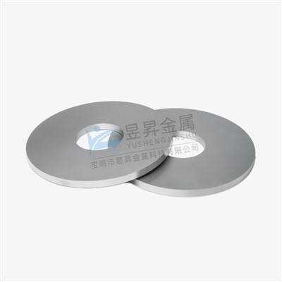
Tantalum sputtering target is a core high‑purity refractory‑metal consumable for physical vapor deposition. It has extremely broad application coverage across electronics‑semiconductor, anti‑corrosion coating, optical‑optoelectronic thin‑film, medical‑device and glass‑coating industries.
In semiconductor IC manufacturing, tantalum targets serve as critical diffusion‑barrier‑layer material for copper‑interconnect processes and are widely adopted by top‑tier chip‑makers for advanced‑node manufacturing. Benefiting from tantalum's excellent biocompatibility, tantalum‑based thin‑films are also applied for medical‑implant coating. Besides, they are used for flat‑panel displays, decorative coating, automotive glass and architectural glass functional thin‑film deposition.
Our tantalum targets are produced complying with GB/T 8182‑2008 standard, with strictly‑controlled metallic‑impurity and gas‑element content. Custom dimensions and shapes are available for both mass‑production‑line and laboratory‑R&D projects.
Product reference link:https://www.tantalumysjs.com/products
Product Parameter Table
Chemical Composition (Weight %, Reference to GB/T 8182‑2008)
| Item | Element | Content(W%) | Remark |
|---|---|---|---|
| Chemical Analysis | Fe | 0.0012 | User‑agreed standard |
| Co | 0.0004 | ||
| Ti | 0.0001 | ||
| Mn | 0.0003 | ||
| Zr | 0.0002 | ||
| Cr | 0.0003 | ||
| Ni | 0.0005 | ||
| Cu | 0.0012 | ||
| Nb | 0.0024 | ||
| W | 0.0045 | ||
| Mo | 0.0033 | ||
| Zn | 0.0003 | ||
| Gas Analysis | C | 0.0035 | |
| N | 0.002 | ||
| H | 0.0005 | ||
| O | 0.0023 |
| General Item | Specification |
|---|---|
| Product Name | Tantalum Sputtering Target |
| Brand | Yusheng Metal |
| Execution Standard | GB/T 8182‑2008 |
| Available Shape | Planar, round, rotary, special‑shaped custom target |
| Purity Grade | 99.95%,99.99% optional |
| Backing Option | Cu / Mo backing plate / tube, bonding service |
| Supply Form | Monoblock or bonded assembly |
Product Advantages & Features
Strict impurity & gas‑element control: Metallic impurities and gas‑components (C, N, H, O) are tightly controlled following GB/T 8182‑2008, lowering particle‑generation risk during sputtering for high‑end semiconductor‑process requirements.
Wide‑range application adaptability: Suitable for semiconductor copper‑barrier‑layer, optical optoelectronic‑film, medical‑implant‑coating, flat‑panel‑display, automotive‑glass and architectural‑glass functional‑coating scenarios.
High‑quality raw‑material guarantee: We adopt premium solid tantalum raw‑material ingots for target fabrication as the foundation of stable finished‑product quality.
Diversified custom capability: Support multiple shapes including planar, round, rotary and special‑shape targets; backing‑plate bonding service is available.
Complete standardized packaging & shipping solution: Mature anti‑oxidation packaging procedure and international‑shipping experience to protect targets from oxidation and mechanical damage.
Inspection & Application
Inspection Methods
Chemical test: ICP for metallic‑impurity analysis; gas‑analysis instrument for C/N/H/O gas‑element detection.
Metallographic inspection: Grain‑size, microstructure and internal‑defect observation.
Dimensional test: Coordinate measuring instrument for dimension, flatness and tolerance verification.
Surface inspection: Roughness test and magnified visual‑inspection for scratches, pits and cracks.
Bond‑strength test for bonded targets.
Main Application
Electronics & Semiconductor: Diffusion‑barrier‑layer material for integrated‑circuit copper‑interconnect technology, adopted in advanced‑process production lines of world‑class chip manufacturers.
Optical & Optoelectronic films: Produce specific‑property optical thin‑films for optical devices, displays and sensors.
Medical devices: Biocompatible coating for medical‑implant components, thin‑film for damaged‑tissue‑repair parts.
Glass‑coating industry: Semiconductor coating, optical coating, decorative coating, flat‑panel‑display, functional coating, automotive glass and architectural‑glass thin‑film deposition.
Our Products

Tantalum Targets.

Tantalum Targets.

Tantalum Targets.
Why Choose Yusheng Metal Tantalum Sputtering Targets?
High‑quality solid tantalum ingot raw‑material input, full‑process manufacturing control from raw‑material to finished‑target, not simple resale of semi‑finished goods.
Strictly implement GB/T 8182‑2008 standard, both metallic‑impurity and gas‑element indicators are well‑controlled for high‑tech‑field usage.
Rich experience for diversified‑scenario demands: semiconductor, medical‑coating, optical‑glass‑coating projects are all covered.
Professional standardized packaging: vacuum‑sealed anti‑oxidation bag, foam cushioning, carton / reinforced wooden‑box options according to order quantity, with clear batch‑number labeling.
Mature international‑logistics arrangement: cooperate with reputable carriers, arrange cargo insurance, pay attention to import‑country customs‑requirements and special‑delivery‑conditions for high‑value sputtering‑target products.
FAQ - Purchasers' Frequently Asked Questions
Q1: What standard do your tantalum sputtering targets follow?
A: Comply with GB/T 8182‑2008 standard; impurity indicators can be further adjusted according to user‑agreed requirements.
Q2: Why use vacuum‑sealed packaging for tantalum targets?
A: Tantalum is susceptible to surface‑oxidation. Vacuum‑sealed packaging effectively prevents oxidation during storage and transportation.
Q3: What packaging forms are available for different order quantities?
A: Small quantity: vacuum‑sealed bag + foam + hard carton. Large quantity: vacuum‑sealed bag + foam + reinforced wooden‑box with fixing strips. Each package is labeled with material name, quantity and batch‑number.
Q4: What are the main application fields of tantalum sputtering targets?
A: Semiconductor integrated‑circuit copper‑interconnect barrier layer, optical optoelectronic‑film, medical‑implant coating, flat‑panel‑display, automotive‑glass and architectural‑glass functional coating etc.
Q5: Can you provide backing‑plate bonding service?
A: Yes, copper or molybdenum backing‑plate / backing‑tube and bonding service are available.
Q6: How do you handle international shipment for tantalum targets?
A: We select reliable carriers, purchase cargo insurance, pay attention to importing‑country customs‑regulations; communicate special‑handling / temperature‑control requirements to carriers for sensitive‑grade targets.
Q7: What test documents can be provided?
A: Material‑test report including metallic‑impurity, gas‑element, dimension and surface‑inspection records can be provided.

Sales Manager:
Contact: Li Fengwu
Email: kd@tantalumysjs.com
Tel: 13379388917
Fax: 0917-3139100
Post code: 721013
Web:https://www.tantalumysjs.com/
Add:Wenquan village Industrial Zone, Gaoxin Development Zone, Baoji City, Shaanxi Province, China
Hot Tags: tantalum targets-wide application, suppliers, manufacturers, factory, customized, buy, price, quotation, quality, for sale, in stock, 95 Pure Ta Tantalum Bar, High Purity Tantalum Targets, cheap Tantalum Bolts, Sputtering Tantalum Targets, Ta Bolt, Tantalum Targets for Semiconductors
Previous
Tantalum Ta Sputtering TargetsYou Might Also Like




Send Inquiry